ASML's secret sauce for semiconductor success amid challenges in the Angstrom Era
TAIPEI, May 22, 2024 /PRNewswire/ — Moore’s Law is not advancing as fast as it used to be under 2nm and even into the Angstrom level, and competitors are trying to catch up. Can ASML, the Dutch semiconductor equipment maker, continue its monopolistic leadership in the extreme ultraviolet (EUV) lithography equipment market?
Will the world’s most advanced high-NA EUV machines be the ultimate weapon for a technological leapfrog for its customers? And how would the geopolitical uncertainties change ASML’s strategy in the future?
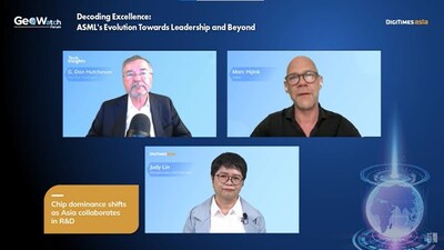
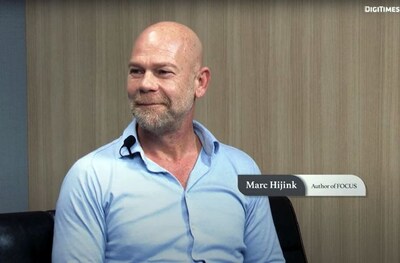
G. Dan Hutcheson, vice chair of TechInsights, who has covered ASML since the 1970s, when it was still a subsidiary of Philips, and Marc Hijink, the author of Focus – the ASML Way and a reporter at Dutch newspaper NRC, joined DIGITIMES Asia for an insightful talk to address these questions.
Navigating geopolitical uncertainties
Although ASML and other semiconductor equipment providers benefit from the demand driven by export controls imposed by the United States to China, geopolitics may have long-lasting implications on the industry as extra capacities and ecosystems are built.
Hutcheson and Hijink see ASML following their customers’ footsteps to decentralize their productions from the Western Pacific corridor to the United States and Europe. Still, the efficiency of its customers’ fab operations may be a concern.
“We’re in a new world where the utilization of the tools is lower,” said Hutcheson, “The problem is, if you can’t find the workers to run the tools or to repair them, keep them running, your wafer fab is useless.”
Hijink observed that Asia will remain an important center for chip production in the future despite the onshoring efforts of various countries and the talent shortage issue since South Korea and Taiwan remain an important part of ASML’s expansion.
ASML’s monopoly status unlikely to be challenged
Yet, Hijink cautioned, “ASML’s biggest fear is that the current restrictions on Chinese technology might even stimulate it in the long term and create an even bigger problem.” He pointed out that the less China gets access to these Western lithography tools, the more the Chinese companies are inclined to build their own. “Even though they might not be able to compete with ASML and Nikon now, you see more room for growth and R&D money in the long term.”
Yet, Hutcheson believes no company can challenge ASML lithography monopoly without massive government subsidies. “Five decades ago, I developed this maxim that the number of unsubsidized competitors a market can sustain is equal to 1/5 the total market size divided by the cost to develop a new generation of technology, and then you subtract 1.5 times that cost,” said Hutcheson. “To attract another competitor in the market, the risk bar must be low enough that there’s enough available R&D to support the development of at least 1.5 more tools than what exists in the market at that time.”
Over those five decades, that maximum is held across 100, or there have been more sub-markets of semiconductor equipment, and that explains the market consolidation of the market from more than 20 semiconductor equipment makers in the 1980s to just a handful right now for lithography, explained Hutcheson.
As a semiconductor industry veteran, Hutcheson witnessed how ASML survived over the past four decades of vicissitudes through better management and technological development. Hijink added that ASML survived because it out-invested in R&D during the low cycles despite being on the brink of bankruptcy several times and cleverly invited its customers TSMC, Intel, and Samsung to invest in it and co-develop the EUV machine.
By getting the investments, ASML managed to get the money to acquire Cymer, the light source company based in San Diego, and establish a strategic alliance with Zeiss, the German lens maker. Those key components and e-beam technology created ASML’s secret sauce of success that competitors cannot copy.
However, repeating such success is getting harder. “No single company can afford to do it alone, as R&D becomes more and more expensive,” Hutcheson quoted John Chen of Nvidia, who was the first R&D president at TSMC, that,” IC no longer means integrated circuit going forward, IC means industry collaboration.”
Hutcheson estimates that the cost of developing a new EUV tool from scratch would require multiple trillions of dollars, which is equal to the Gross Domestic Product for some countries, and that’s assuming that one gets around all the IP barriers in place. “To some extent, it levels the geopolitical playing field. So maybe EUV should receive the Nobel Peace Prize because no country can attack any other country unless they have the EUV,” quipped Hutcheson.
Can high-NA machines help technology leapfrog?
As Intel, Samsung, and TSMC are aiming to mass produce 2nm chips in the next few years and advance towards 1.4-1.6 nm, the ASML’s high-NA EUVs are making the headlines of semiconductor industry newspapers.
As always, ASML ships the US$300 million High-NA machines to customers according to the timetable agreed with customers and does the laborious adjusting and error corrections with customers. The media has been describing high-NA EUVs as the key for technology catch-uppers to leapfrog the incumbent. However, Hutcheson delved deeply into the intricacies involved in the complex processes of semiconductor manufacturing beyond lithography.
“There’s a lot of technology issues in the 2nm and 1.4nm era. And we will have to see if they can pull it off and turn it into an advantage,” Hutcheson explained that lithography is not the only factor at stake, there are also issues with the gate-all-around (GAA) structures, due to the leakage problems with that. “There’s also reliability problems, and the epitaxial layer is pretty poor. So really, there are more material and systems engineering problems than lithography problems.”
Though Intel has seemingly bought up all available high-NA machines for the year, TSMC is not in a hurry to apply it to its 1.4-1.6nm process. However, ASML said all of their customers who have bought EUVs are going to upgrade to High-NA EUVs.
“I think that Intel has to do more, try to leapfrog TSMC, which is a daring move, but that’s just one part of Intel’s challenge,” said Hijink. “Their biggest challenge is not the technology, but the fact that they want to do foundry business because they have to create enough wafer footprint or enough scale to be economically viable with huge competitors like Samsung and TSMC. So that adds to the problem of adopting a new technology where they’re not as experienced.”
Hutcheson cautioned that it is too early to judge the outcome of technology competitions. Yet seeing from the history of the semiconductors industry, decades of research, blood, sweat, and tears, and fixing tons of errors, plus making the right decisions at the right timing and building deep trust with customers made ASML and TSMC what they are today.
ASML, a blend of European, Asian, and American cultures as the result of acquisitions, can be a great teacher for TSMC, which is just starting to expand its footprints to the US and Europe. With such a close bond between the two, with AI being the main driving force for semiconductor’s future growth, one can be sure there will not be short of fascinating stories in the future.
Editor’s note: For more insights and analysis from Hutcheson and Hijink on the industry, watch DIGITIMES Asia’s new GeoWatch video, ‘Decoding Excellence: ASML’s Evolution Towards Leadership and Beyond.’ Click the link here to access this informative video: https://dgt.ms/geowatch0516
![]() View original content to download multimedia:https://www.prnewswire.com/news-releases/asmls-secret-sauce-for-semiconductor-success-amid-challenges-in-the-angstrom-era-302152529.html
View original content to download multimedia:https://www.prnewswire.com/news-releases/asmls-secret-sauce-for-semiconductor-success-amid-challenges-in-the-angstrom-era-302152529.html
SOURCE DIGITIMES ASIA


 Private Internet Access gives you unparalleled access to thousands
of next-gen servers in over 83 countries and each US state. Your
VPN experience will always be fast, smooth, and reliable.